INTRODUCTION OF DIGITAL LOGIC
Digital logic is
the fundamental concept underpinning all modern computer systems. Put simply,
it’s the system of rules that allow us to make extremely complicated decisions
based on relatively simple “yes/no” questions.
· COMBINATIONAL LOGIC
1)
A logic block contains no memory and computes the output given the
current inputs.
2)
Can be defined in three ways:
a)
Truth Table – the truth table shows many
possible combination of input values, in tabular from between the input values
and the result of a specific Boolean operator or combinations on the input
variables.
b)
Graphical Symbols – the layout of connected gates that
represent the logic circuit
a)
Boolean Equation – Boolean function that consist
possible combination of inputs that produce an output signal
(1)
Examples:
· BOOLEAN QUATION FORM
A Boolean algebra is the
combination of variables and operators. Typically it has one or more inputs and
produces an output in the range of 0 – 1. The complement of a variable is shown
by a bar over the letter.
All Boolean equation can be
represented in two forms:
1) Sum-of-product (SOP)
a) Combination of input values that produces 1s is convert into equivalent
variables, AND-ed together then OR-ed together with others combination
variables with the same output.
SOP
is easier to derived from truth table.
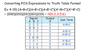
1) Product-of-sum (POS)
a) Input combination that produces 0s in sum terms ( OR-ed variables) are
AND-ed together.
b) Convert input that produces 0s into equivalent variables, OR-ed
variables, then AND-ed with other OR-ed variables.
· SIMPLIFICATION OF BOOLEAN EQUATION
There are two ways to simplify Boolean equation,
Laws of Boolean Algebra and Karnaugh Map.
·
Laws of Boolean Algebra – rules to simplify Boolean
expression
·
Karnaugh Map – A grid-like representation of a
truth table
· Laws of Boolean Algebra
Boolean
expressions can be simplified or manipulated. Table below shows the basic rules
of Boolean Algebra to help manipulating logic equations.
·
Karnaugh
Map
The
Karnaugh map provides a simple and straight forward method of minimizing
Boolean expressions. The only limitation is that it will be ineffective for
more than 4 inputs.
The
Karnaugh map can also be describe as a grid like representation of a truth table.
The rows and columns corresponds to the possible values of the function inputs.
A product
term that includes all of the variables once, either complimented or not
complemented is called a minterm. For example, if there are two input values A
and B, there are four minterms A’B’, A’B , AB’, AB, which represent all of the
possible input combinations for the function.
EXAMPLE OF MINTERMS
Karnaugh
map can be applied to expressions of more than two variables. We simply extend
Karnaugh map for two variables to three variables as indicated in the above
figure.
·
GROUPING
1’S IN KARNAUGH MAP
a)
The group can only contain 1s.
b)
Only 1s adjacent cells can be grouped; diagonal
grouping is not allowed.
c)
The number of 1s in a group must be a power of 2,
means a group can contain 2,4,8,16 of 1s.
d)
The group must be as large as possible while still
following all rules.
e)
All 1s must belong to a group, even if it is a
group of one.
f)
Overlapping groups are not allowed
g)
Use the fewest number of groups possible
·
SIMPLIFIED
EQUATION TO LOGIC CIRCUIT
I.
A SYMBIOSIS PROCESS: for every Boolean expression
there is a logic circuit, and for every logic circuit there is a Boolean
expression.in other words, we can derive the other if we have one of them.
II.
Simplifien L2 is represented into logic circuit
III.
From the L2 equation the SOP equation is the input
for L2 (output). There are 3 inputs s1,s2, and s3 where 2 input will be AND-ed
and OR-ed with 2 AND gates.
IV.
If any other 2 AND gate variables such as AB +
A’C,we still use 3 inputs,A,B and C as A’ can be represented using an inverted
A.
V.
Figure below shows the logic circuit that represent
L2 function
·
UNIVERSAL
GATES
Gates that can be
used to implement any gates ;ike AND, OR and NOTor any combination of these basic gates are called universal
gates. NAND and NOR are such examples.
I.
NAND GATE
A NAND gate is a
logic gate which produce an output that false only if all of its inputs are
true. Figure below shows the truth tableand graphical symbol of NAND gate.
I.
NOR GATE
A NOR gate is a
logic gate which produces a high output (1) results if both the inputs to the
gate are LOW(0); a LOW output (0) results if are both inputs is HIGH (1).
Figure below shows the truth table and graphical symbol for NOR gate.


No comments:
Post a Comment